Location:Home Page > Archive Archive
Principal analysis of BUCK / BOOST circuit, a summary is also in place
2023-03-18【Archive】
Dollar Converter
Also known as a buck converter, this is a single-tube non-isolated DC-DC converter whose output voltage is lower than input voltage.
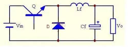
In figure, Q represents switching tube, and its control voltage is usually a PWM (pulse, pulse width, pulse width modulation) signal. The signal period is Ts, then signal frequency is f=1/Ts, conduction time is Ton, off time is Toff, then period is Ts=Ton+Toff, duty cycle is Dy=, Ton/Ts.
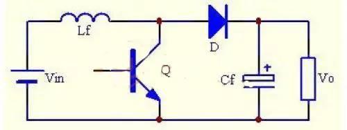
Accelerated Converter
Also known as a boost converter, this is a single-tube, non-isolated DC/DC converter whose output voltage is higher than input voltage.
The switching tube Q is also PWM controlled, but maximum duty cycle Dy must be limited and it cannot work in Dy=1 state. The inductor Lf is at input and is called step-up inductor. The Boost converter also has two modes of operation: CCM and DCM.
Up/Down Converter
Also known as a buck-boost converter, this is a single-tube non-isolated DC-DC converter whose output voltage can be lower or higher than input voltage, but output voltage polarity is opposite to input voltage. The Buck/Boost converter can be thought of as a Buck converter and a Boost converter connected in series, and switching tube is combined.
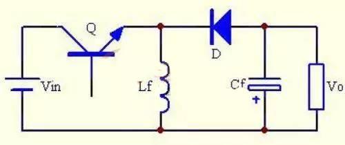
The Buck/Boost converter also has two modes of operation, CCM and DCM, and Q switching tube is also PWM controlled.
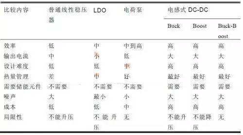
LDO Characteristics
① Very low input-output voltage difference
② Very little internal loss
③ Slight temperature drift
④ High output voltage stability
⑤ Very good load and line adjustment
⑥ Wide operating temperature range
⑦ Wide input voltage range
⑧ The peripheral circuit is very simple and convenient to use
DC to DC conversion is conversion of a fixed DC voltage to an AC DC voltage, also known as DC interruption. There are two chopper operation modes, one is pulse width modulation mode, Ts is unchanged and ton is changed (common), and other is frequency modulation mode, ton is unchanged and Ts is changed (light). interfere). His specific schema consists of following categories:
(1) A step-down circuit is a step-down chopper whose average output voltage U0 is less than input voltage Ui and has same polarity.
(2) The booster circuit is a step-up chopper, its average output voltage U0 is greater than input voltage Ui, and polarity is same.
(3) Buck-Boost circuit - step-down or step-up chopper whose average output voltage U0 is greater or less than input voltage Ui, polarity is reversed, inductance is transferred.
(4) The Cuk circuit is a step-down or step-up chopper, its average output voltage U0 is greater or less than input voltage Ui, polarity is reversed, and capacitance is transferred.
DC-DC is divided into three types of DC-DC: BUCK, BUOOST and BUCK-BOOST. Among them, DC-DC type BUCK can only step down, and step down formula is: Vo=Vi*D
BOOST type DC-DC can only boost voltage, boost formula: Vo=Vi/(1-D)
BUCK-BOOST DC-DC type, can boost or boost, formula: Vo=(-Vi)* D/(1-D)
D is charge duty cycle, i.e. conduction time of MOSFET, 0 <1.
The efficiency of switching regulated power supply is very high, but output ripple voltage is high, noise is large, and performance of voltage regulation speed is also low, especially when it supplies power to analog circuit, it will have a greater impact.
Due to high efficiency of switching power supply, it can usually reach more than 80%, so when choosing its output current, it is necessary to accurately measure or calculate maximum absorption current of electrical equipment, so that selected switching power supply has a high performance Price ratio, usual formula output power calculation: Is=KIf where: Is - rated output current of switching power supply, If - maximum current consumption of electrical equipment, K - safety factor, usually from 1.5 to 1.8.
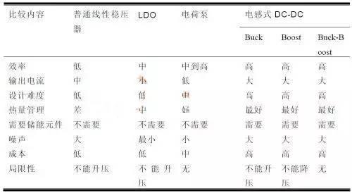
Capacitive switching power supply
They can step up or step down input voltage, and can also be used to create a negative voltage. Its internal FET switch matrix controls charging and discharging of flying capacitors in a certain way, so that input voltage is multiplied or decreased by a certain factor (0.5, 2, or 3) to obtain desired output voltage. This special modulation process can guarantee an efficiency of up to 80%, requiring only external ceramic capacitors. As circuit switches, charge pump structure will also generate certain output ripple and electromagnetic interference (EMI). Energy is first stored and then released in a controlled manner to produce desired output voltage.
Related
- Principal analysis of BUCK / BOOST circuit, a summary is also in place
- Experience in recognition of circuit diagrams of electronic circuits and method of circuit analysis
- Analysis of power circuit of a classic single-chip microcomputer
- Analysis of damping RC circuit of a switching power supply "haberdashery"
- Circuit Analysis of 6 Examples Explaining Lightning Surge Protection in Detail
- What does inside of a multilayer PCB look like? Three-dimensional general analysis of design process of high-quality printed circuit boards
- What is a delay scheme? Explanation of 6 Kinds of Delay Circuit Principles
- Three circuit diagrams to teach you how to understand how a buck RC works
- What is purpose of connecting a polar capacitor and a non-polar capacitor in parallel?
- Four Tricks to Make Your Boost Circuit Safer
Hot Posts
 How to distinguish induction from leakage, we will teach you three tricks! Ordinary people can also learn super practical
- What is drowning in gold? Why Shen Jin?
- This is a metaphor for EMI/EMS/EMC that can be understood at a glance.
- How many types of pads have you seen in PCB design?
- Summary of Common PCB Repair Techniques
- What is three anti-paint? How to use it correctly?
- Knowing these rules, you will not get confused looking at circuit diagram.
- How to make anti-interference PCB design?
- Can diodes do this?