Location:Home Page > Archive Archive
Still foolishly setting silkscreen bit numbers of PCB components one by one?
2023-03-27【Archive】
For subsequent assembly of components, especially manual assembly of components, PCB assembly drawing is usually used to place and position components. At this time, silkscreen position number indicates its need.
Friends starting to draw circuit boards should have such an operation. Manually setting bit numbers of silkscreen components one by one is very tedious and inefficient...
Is there a good solution?
During production, silkscreen bit number on PCB can be displayed or hidden, but this does not affect output of assembly drawing. Press "L" shortcut key, click close all layers button, that is, close all layers, and then mark only silkscreen layer and corresponding solder mask layer to open, and then silkscreen can be adjusted.
The following are principles and generally accepted recommended sizes for customizing silkscreen item number:
(1) The silkscreen item number is not listed on soldermask, and it is missing after silkscreen production is placed.
(2) The silkscreen position number is clear and recommended font size is 4/25 mil, 5/30 mil, 6/45 mil width/height.
(3) Keep same direction. As a general rule, there should not be more than two directions on a PCB. It is recommended that letters be on left or bottom, as shown in Figure 11-21.
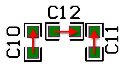
Figure 11-21 Silkscreen number display direction
(4) Some of silkscreen marks on left and right sides can be marked with 2D guide lines or squares for easier reading, as shown in fig. 11-22.
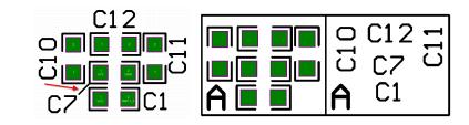
Figure 11-22 Auxiliary lines and squares
Silkscreen number setting method
AltiumDesigner provides a quick silkscreen setup method, ie "Component Text Position" function, which can quickly place a component's silkscreen around a component or in center of a component.
(1) Select a component to control.
(2) Press shortcut key "AP" to open "Component Text Position" dialog box, as shown in Figure 11-23, dialog box provides two placement methods: "ID" and "Comment". Here, "Identifier" is taken as an example for illustration purposes.
(3) "Identifier" provides multiple directions up, down, right, left, up left, down left, up right, and down right, which can correspond to number keys on a small keyboard. After setting keyboard shortcut for Component Text Position command, if you want it to quickly place silkscreen position number of selected component on top of component, press number keys "5" and "2" on small keyboard. Perform this operation as shown in Figure 11-24. Other directions are similar. For example, press number keys "5" and "6" to place component to right of component, and press number keys "5" and "8" to place it below component.
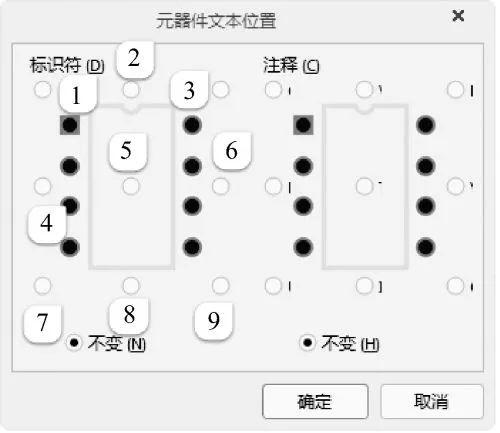
Figure 11-23 Component Text Position Dialog Box
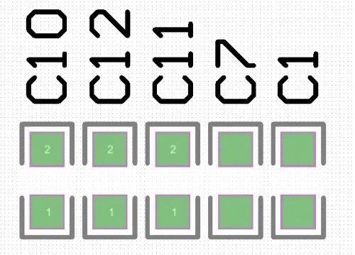
Fig. 11-24. Quickly place silkscreen label on top of component
Some tips for PCB design
1. How to choose PCB material?
PCB selection should strike a balance between design compliance, mass production, and cost. Design requirements include both electrical and mechanical components. Usually this material issue becomes more important when designing very high speed PCBs (above GHz). For example, currently widely used FR-4 material may not be suitable for use, since dielectric losses at a frequency of several GHz will greatly affect signal attenuation. With regard to electricity, it is necessary to pay attention to whether permittivity (permittivity) and dielectric loss are suitable for design frequency.
2. How to avoid high frequency interference?
The main idea of RF interference prevention is to minimize interference of high frequency signal electromagnetic fields, which is so-called crosstalk (Crosstalk). You can increase distance between high speed signal and analog signal, or add a ground/shunt trace next to analog signal. Also note digital ground noise interference with analog ground.
3. How to solve problem of signal integrity in high-speed PCB design?
Signal integrity is mainly dependent on impedance matching. Factors that affect impedance matching include source structure and output impedance, trace characteristic impedance, load end characteristics, and trace topology. The solution is to rely on termination and adjust wiring topology.
4. Can a ground wire be added between differential signal lines?
In general, a ground wire cannot be added in middle of a differential signal. Because most important point of differential signal application principle is to use advantages brought by mutual coupling (coupling) between differential signals, such as suppression of flow, anti-noise (noise immunity) ability and so on. If a ground wire is added in middle, coupling effect will be destroyed.
5. Do I need to add earth wire shielding on both sides when distributing clocks?
The need to add a shielded ground wire depends on crosstalk/EMI situation on board, and if shielded ground wire is not properly handled, it can make things worse.
6. What to do with line segments (with smallrectangle) that appear in Allegro wiring?
The reason for this is that after using module again, an auto-named group is automatically created, so key to solving this problem is to split group again, select group in hosted state, and split. After executing this command, move all lines of small rectangles and touch ix00 coordinate.
7. How to best meet EMC requirements without putting undue pressure on costs?
The increase in cost due to EMC on PCB is usually associated with an increase in number of ground layers to enhance shielding effect and addition of ferrite beads, chokes and other high frequency harmonic suppression devices. In addition, it is usually necessary to interact with shielding structures through other mechanisms in order for entire system to comply with EMC requirements. The following are just some of PCB design techniques to reduce effects of electromagnetic radiation from circuit:
1) Select a device with a slower signal slope (slew rate) to reduce high frequency components generated by signal.
2) Pay attention to placing high-frequency components not too close to external jacks.
3) Pay attention to match impedance of high-speed signals, wiring layer and its return current path (return current path) to reduce high-frequency reflection and radiation.
4) Place enough suitable decoupling capacitors on power pins of each device to mitigate noise on power and ground planes. Pay particular attention to whether frequency response and temperature response of capacitor are within design requirements.
5) The ground near external connector can be properly separated from formation, and ground of connector must be connected to hull ground nearby.
6) Ground guards/shunt tracers can be used correctly around some particularly high speed signals. But pay attention to effect of guard/shunt traces on impedance of trace.
7) The power layer is 20H smaller than ground, and H is distance between power layer and ground.
8. What rules should be observed when designing high frequency PCBs above 2G and microstrip?
To design RF microstrip lines, it is necessary to use 3D field analysis tools to extract transmission line parameters. All rules must be specified in this field extraction tool.
9. Which end is better for AC coupling a high speed PCB signal?
I often encounter different processing methods, some near receiving end and some near transmitting end.
Let's first look at role of condensateAC couplers, no more than three points: ① DC source and sink are different, so DC blocking;
②There may be crosstalk in DC component during signal transmission, so DC blocking improves signal's eye diagram;
③AC coupling capacitors can also provide DC bias and overcurrent protection.
Ultimately, role of AC coupling capacitor is to provide DC bias, filter DC component of signal, and ensure that signal is symmetrical about 0-axis.
Then why add this AC coupling capacitor? Of course, there are benefits: adding AC coupling capacitors will certainly improve coupling between two stages and can improve noise margin. Be aware that AC-coupling capacitors are typically breaking point in high-speed signals and cause signal edges to slow down.
1) Some conventions or guidelines will specify design requirements and we will post them according to requirements of design guide.
2) There is no requirement in first article. If it is IC to IC, please place it closer to receiving side.
3) If chip is connected to socket, place it closer to socket.
10. How do you check if a PCB meets requirements of design process when it leaves factory?
Many PCB manufacturers must run a Power-On Network Continuity Test before PCB processing is complete to ensure all connections are correct. At same time, more and more manufacturers are also using X-ray inspection to check for some defects during etching or laminating. To check finished board after patch processing, ICT test is usually used, which requires addition of ICT test points during PCB design. In event of a problem, a special x-ray inspection device can also be used to rule out whether problem is due to processing.
Related
- Still foolishly setting silkscreen bit numbers of PCB components one by one?
- The most complete test of iron 5 processes, one less will not work
- Haberdashery|General failure mechanism and analysis of electronic components
- Summary of Common PCB Repair Techniques
- Understand Current Detection Circuit in One Article
- One Article for Understanding PFC (Power Factor Correction)
- Diode switching circuit and troubleshooting, one complete wizard
- Diagram of relationship between PCB layout and EMC
- One article eats up all rectifier and filter circuits
- Why do diodes conduct electricity in one direction? understand in seconds
Hot Posts
 How to distinguish induction from leakage, we will teach you three tricks! Ordinary people can also learn super practical
- What is drowning in gold? Why Shen Jin?
- This is a metaphor for EMI/EMS/EMC that can be understood at a glance.
- How many types of pads have you seen in PCB design?
- Summary of Common PCB Repair Techniques
- What is three anti-paint? How to use it correctly?
- Knowing these rules, you will not get confused looking at circuit diagram.
- How to make anti-interference PCB design?
- Can diodes do this?