Location:Home Page > Archive Archive
Haberdashery|General failure mechanism and analysis of electronic components
2023-03-27【Archive】
The main failure modes of electronic components include, but are not limited to, open circuit, short circuit, fire, explosion, leakage, functional failure, electrical drift, intermittent failure, etc. For iron engineers, failure of electronic components is very troublesome business, for example, if a semiconductor device looks good, but in fact is half or completely out of order, it will take a long time to debug hardware circuit, and sometimes even machine will explode.
Equipment engineer debugging explosion site
Therefore, knowledge of effective mechanism and characteristics of various electronic components is indispensable knowledge for hardware engineers. The following classification details failure modes and mechanisms of various electronic components.
1 Types and mechanisms of resistor failure
Failure mode. Various failure phenomena and their manifestations.
Failure mechanism is a physical, chemical, thermodynamic, or other process that leads to failure.
01 Types and mechanisms of resistor failure
▶Open circuit: The main failure mechanism is that resistance film burns or falls off over a large area, substrate breaks, and lead cap and resistance body fall off.
▶Resistance drift out of specification: resistive film damaged or damaged, there are mobile sodium ions in substrate, poor protective coating.
▶Breakage of lead wires: defects in welding process of resistor body, contamination of solder joints, mechanical damage to lead wires.
▶Short circuit: silver migration, corona discharge.
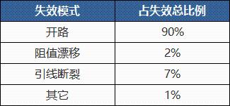
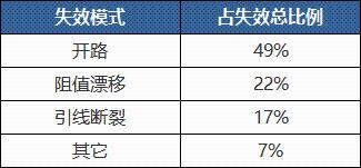
02 Table of ratio of failure mode to total number of failures
▶Wirewound resistors:
▶Non-wire resistors:
03 Failure mechanism analysis
The failure mechanism of resistors is multifaceted, and resistor aging is caused by various physical and chemical processes occurring under operating or environmental conditions.
▶Structural changes in conductive materials:
The conductive film layer of thin film resistors is usually obtained by vapor deposition, and to a certain extent it has an amorphous structure. From a thermodynamic point of view, an amorphous structure tends to crystallize. Under operating or environmental conditions, amorphous structure in conductive film layer tends to crystallize at a certain rate, that is, internal structure of conductive material tends to densify, which can often cause resistance value to drop. The rate of crystallization increases with increasing temperature.
The resistive wire or resistive film will be subjected to mechanical stress during preparation process, which will distort its internal structure. The smaller diameter of wire or thinner film layer, greater effect of stress. Generally, heat treatment can be used to eliminate internal stress, and residual internal stress can be gradually eliminated during long-term use, and resistance value of resistor can be changed accordingly.
The crystallization process and internal stress relief process slow down over time, but are unlikely to stop over life of resistor. These two processes can be considered to proceed at approximately constant rate during duty cycle of resistor. The associated change in resistance value is a few thousandths of original resistance value.
High temperature aging of electrical load: In any case, electrical load will accelerate aging process of resistor, and effect of electrical load on accelerated aging of resistor will be more significant than accelerated aging at elevated temperature. , because body of resistor is in contact with lead cap. Part of temperature rise is greater than average temperature rise of resistor. As a rule, each time temperature rises by 10°C, service life is halved. If, due to overload, temperature rise of resistor exceeds temperature rise by 50°C at rated load, life of resistor is only 1/32 of normal life. The stability of resistor for 10 years can be assessed using accelerated life tests in less than four months.
DC load electrolysis: Under influence of a DC load, electrolysis causes resistor to age. Electrolysis occurs in groove of grooved resistor, and alkali metal ions contained in resistor matrix move in electric field between grooves, creating an ionic current. In presence of moisture, electrolysis process proceeds more intensively. If resistance film is carbon film or metal film, it is mainly electrolytic oxidation; if resistance film is an ox filmIda metal, it is mainly electrolytic reduction. For high resistance film resistors, effects of electrolysis can increase resistance value and damage to film along one side of groove spiral can occur. Carrying out a direct current load hot flash test can comprehensively evaluate anti-oxidation or anti-reduction performance of resistor base material and film layer, as well as moisture-proof performance of protective layer.
Typical sample view
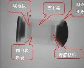
There is a gap in surface electrode
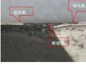
Discontinuous ribbon-like voids in surface layer of electrolytic silver
▶Vulcanization:
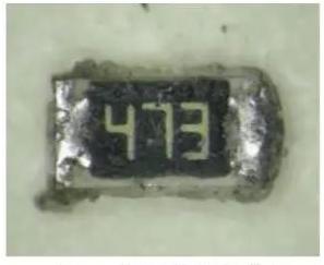
After a batch of field instruments was used in a chemical plant for a year, instruments failed one after other. After analysis, it was found that resistance value of thick-film chip resistor used in instrument became larger and even became an open circuit. Putting a failed resistor under a microscope, you can find that a black crystalline substance appears on edge of resistor electrode, further analysis of composition of which shows that black substance is a silver sulfide crystal. It turned out that resistor was corroded by sulfur from air.
▶Gas adsorption and desorption:
The resistive film of a film resistor can always absorb a very small amount of gas at interface between grains or conductive particles and bonding part, which constitute intermediate layer between grains and prevent interaction between conductive particles. contact, thereby significantly affecting resistance value.
Synthetic film resistors are manufactured under normal pressure. When operating in vacuum or low pressure, desorbed part will be attached to gas, which will improve contact between conductive particles and reduce resistance value. Similarly, when thermally decomposed vacuum-made carbon film resistors are operated directly under normal ambient conditions, they will absorb some of gas due to increase in air pressure, which will increase resistance value. If unmarked semi-finished product is preliminarily kept at normal pressure for proper time, resistance stability of finished resistor will improve.
Air temperature and pressure are main environmental factors affecting gas adsorption and desorption. With physical adsorption, a decrease in temperature can increase equilibrium adsorption capacity, and vice versa with an increase in temperature. Because adsorption and desorption of gas occur on surface of resistor. Therefore, effect on film resistors is more significant. The resistance value can vary by 1%~2%.
▶Oxidation:
Oxidation is a long-term factor (unlike adsorption). The oxidation process starts from surface of resistor and gradually goes deeper. With exception of film resistors made of noble metals and alloys, resistors made of other materials will be attacked by oxygen in air. Oxidation leads to an increase in resistance. The thinner resistive film, more noticeable effect of oxidation.
The main measure to prevent oxidation is sealing (metal, ceramic, glass and other inorganic materials). Coating or sealing with organic materials (plastics, resins, etc.) cannot completely prevent permeability of protectivelayer for moisture or air, and while it may slow down oxidation or absorb gases, it will also create some new problems associated with organic protective layer. aging factors.
▶Influence of organic protective layer:
During formation of organic protective layer, volatile polycondensation products or solvent vapors are released. During heat treatment process, some volatile substances diffuse into resistor body, which leads to an increase in resistance value. Although this process can take 1 to 2 years, time to significantly affect resistance value is 2 to 8 months. In order to ensure resistance value of finished product is stable, it is more appropriate to put product in warehouse for a certain period of time before leaving factory.
▶Mechanical damage:
The reliability of a resistor largely depends on its mechanical properties. Resistor case, lead cap and lead wire must have sufficient mechanical strength Defects in substrate, damage to lead cap or broken leads can lead to failure of resistor.
2 Electrolytic capacitor failure
01 Exhaustion Error
▶First explanation
Usually, end of life of an electrolytic capacitor is judged by fact that capacity drops below 80% of nominal value (initial value). Due to electrolyte filling of first aluminum electrolytic capacitors, capacity of aluminum electrolytic capacitors slowly drops in early stages of operation. Since working electrolyte continuously repairs anodic oxide film damaged by impurities during loading process, electrolyte is gradually reduced. At end of use, due to reduction of electrolyte volatilization, electrolyte with increased viscosity hardly comes into full contact with oxide film layer on surface of rough aluminum foil after corrosion treatment, which reduces effective area of the aluminum electrolytic capacitor plate, that is, capacity of anode and cathode aluminum foil decreases. , causing a sharp drop in capacitance. Therefore, we can assume that decrease in capacitance of aluminum electrolytic capacitor is caused by volatilization of electrolyte. The most important cause of electrolyte volatilization is high ambient temperature or heat.
▶Second explanation
The reason for heating of aluminum electrolytic capacitors due to operating conditions is ripple (or ripple) of current of aluminum electrolytic capacitors during their operation in rectification and filtering modes (including high-frequency rectification and filtering output of a switching power supply) and bypass power supply of electric furnaces Flow through aluminum electrolytic capacitor causes loss in ESR of aluminum cellcontrol condenser and converts it into heat to generate heat.
When electrolyte of aluminum electrolytic capacitors evaporates more and solution becomes thicker, resistivity increases due to increase in viscosity, which increases equivalent series resistance of working electrolyte, resulting in a significant increase in capacitor loss and loss angle. . For example, for an electrolytic capacitor with an operating temperature of 105 degrees, when maximum temperature of core case is higher than 125 degrees, viscosity of electrolyte increases sharply, and ESR of electrolyte increases by almost ten times. .Increased equivalent series resistance will generate more heat, resulting in more electrolyte volatilization. This cycle goes on and on, and capacity of aluminum electrolytic capacitor drops sharply and may even lead to an explosion.
▶Third Interpretation
Increased leakage current often causes aluminum electrolytic capacitors to fail. Excessive applied voltage and excessive temperature will cause an increase in leakage current.
02 Pressure relief device operation
To prevent electrolyte explosion in aluminum electrolytic capacitor caused by internal high pressure caused by internal high temperature boiling gas or gas generated by electrochemical process. In order to prevent explosion of aluminum electrolytic capacitors, aluminum electrolytic capacitors with a diameter of more than 8 mm are equipped with pressure relief devices that operate before air pressure inside aluminum electrolytic capacitor reaches a dangerous value, but does not cause an explosion of aluminum electrolytic capacitor. When pressure relief device of aluminum electrolytic capacitor is triggered, aluminum electrolytic capacitor is declared invalid.
▶Aluminum electrolytic capacitor pressure relief device (cross in middle)
▶An electrochemical process triggers a pressure relief device
The leakage current of aluminum electrolytic capacitors is an electrochemical process that has been discussed in detail above and will not be repeated. The electrochemical process will generate gas, and accumulation of these gases will cause internal air pressure of aluminum electrolytic capacitor to rise, and finally reach pressure release device to release pressure.
▶Excessive temperature triggers pressure relief device
The temperature of aluminum electrolytic capacitor is too high, which may be due to high ambient temperature. For example, there are heating elements near aluminum electrolytic capacitor, or entire electronic device is in a high temperature environment;
The second reason why aluminum electrolytic capacitor temperature is too high is because temperature of core case is too high. The main reason for high case temperature of aluminum electrolytic capacitors is excessive ripple current flowing through aluminum electrolytic capacitors. Excessive current ripple causes excessive ESR loss of aluminum electrolytic capacitor, and excessive heating causes electrolyte to boil to form a large amount of gas, which causes internal pressure of aluminum electrolytic capacitor to rise sharply and pressure relief device to operate.
03 Instant Overheat
Typically, every 10°C drop in core temperature of an aluminum electrolytic capacitor doubles its life. This core is located approximately in center of capacitor and is hottest point inside capacitor. However, when capacitor is heated to its maximum allowable temperature, for most types of capacitors at 125°C, electrolyte will be moved by capacitor case, resulting in a 10 times increase in ESR of capacitor. With this effect, instantaneous overheating or overcurrent can permanently increase ESR, causing capacitor to fail. When using high temperatures and high ripple currents, special attention should be paid to possibility of instantaneous overheating, and special attention should be paid to cooling of aluminum electrolytic capacitors.
04 Generating transient overvoltages
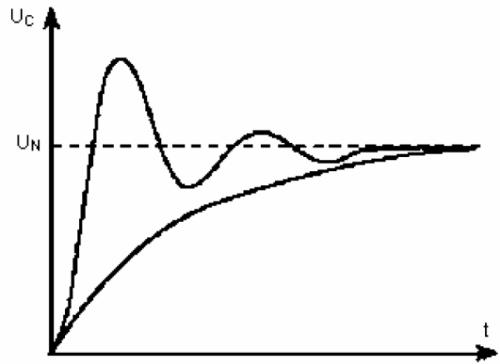
▶Power on shock
During power-up, due to release of energy stored in filter inductor, filter capacitor is momentarily overvoltaged into filter capacitor.
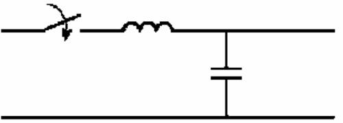
Power-on overvoltage protection circuit
▶Precautions against capacitor overvoltage
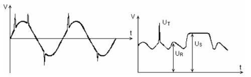
Capacitors fail easily under overvoltage conditions, and instantaneous high voltages often occur in practical applications.
Choose aluminum electrolytic capacitors with good transient overvoltage resistance. RIFA aluminum electrolytic capacitors provide parameters for instantaneous overvoltage values.
05 Electrolyte dryness is main cause of aluminum electrolytic capacitor failure
The reason electrolyte is dry is because electrolyte naturally volatilizes and electrolyte is consumed.
▶Electrolyte naturally volatilizes
The rate of electrolyte evaporation increases with increasing temperature
The evaporation rate of electrolyte is related to sealing quality of capacitor, which must have good sealing performance regardless of high or low temperature.
▶Electrolyte consumption
The electrochemical effect caused by leakage current consumes electrolyte, and service life of aluminum electrolytic capacitor decreases as leakage current increases.
Leakage current increases with temperature: Leakage current at 25°C is only one tenth of leakage current at 85°C. Leakage current increases with applied voltage: aluminum electrolytic capacitor with a withstand voltage of 400V Leakage current at rated voltage of about 5 times leakage current at 90% of rated voltage.
06 Electrolyte drying affects life of aluminum electrolytic capacitors
▶Factors Affecting Service Life of Aluminum Electrolytic Capacitors: Temperature
According to different electrolytes of aluminum electrolytic capacitors, maximum working temperature of aluminum electrolytic capacitors can be divided into:
General purpose, 85℃
General use at high temperatures, 105℃
Special application at high temperatures, 125℃
Car engine compartment, 140~150℃
If temperature rises by 10°C, service life will be halved.
▶Factors Affecting Service Life of Aluminum Electrolytic Capacitors: Rated Life Hours
Aluminum electrolytic capacitors can be divided into:
General Purpose (Normal Temperature, 3 years), 1000 hours
General use (normal temperature, hopefully long term), over 2000 hours
●Industrial grade, extended life
▶Factors Affecting Service Life of Aluminum Electrolytic Capacitors: Electrolyte
The amount of electrolyte determines service life of aluminum electrolytic capacitors.
▶Factors affecting service life of aluminum electrolytic capacitors: application conditions
High temperature shortens life of aluminum electrolytic capacitors, high ripple current shortens life of aluminum electrolytic capacitors, high operating voltage shortens life of aluminum electrolytic capacitors.
07Parameters and application conditions affecting service life of aluminum electrolytic capacitors
▶Relationship between operating voltage and leakage current
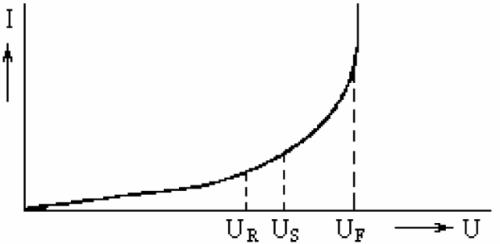
Relationship between operating voltage and leakage current
The relationship between leakage current and applied voltage of a 450V/4700uF/85℃ aluminum electrolytic capacitor produced by a certain company is as follows:
▶Relationship between temperature and leakage current
The relationship between leakage current and ambient temperature of a 450V/4700uF/85℃ aluminum electrolytic capacitor produced by a certain company is as follows:
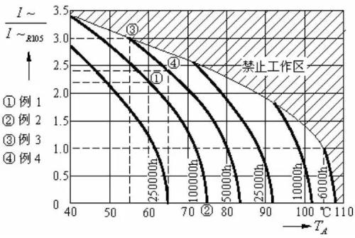
▶The effect of temperature, voltage and ripple on life expectancy
Let's take an aluminum electrolytic capacitor for electronic ballast as an example.
The service life of aluminum electrolytic capacitors is different under different voltage and temperature conditions, table is as follows:
Derating characteristics of aluminum electrolytic capacitor used in electronic ballast as shown in figure below:
The service life of aluminum electrolytic capacitor used in electronic ballast under overvoltage is as follows:
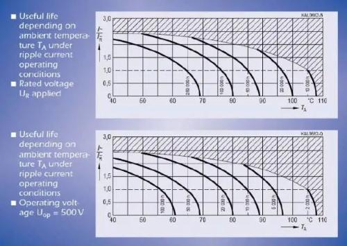
The relationship between aluminum electrolytic capacitor life, temperature and ripple current is as follows:
3 Inductor failure analysis
Inductor failure mode: inductance and other performance, open circuit, short circuit.
Failure mechanism of molded wirewound inductor:
The mechanical stress created by magnetic core during processing is relatively large and cannot be removed;
There are impurities in magnetic core or material of hollow core itself is inhomogeneous, which affects state of magnetic field of magnetic core and leads to a deviation in magnetic permeability of magnetic core;
●Due to cracks after sintering;
When connecting a copper wire and a copper strip by dip soldering, part of coil is splashed with tin liquid, which melts insulating layer of enameled wire and causes a short circuit;
Copper wire is thin, and when it is connected to a copper strip, it can lead to false welding and open circuits.
01 Solder resistance
After reflow soldering, sensitivity of low frequency chip is increased by 20%.
Because temperature of reflow soldering exceeds Curie temperature of inductive material of low frequency chip, demagnetization occurs. After chip is demagnetized, magnetic permeability of chip material returns to its maximum value, and inductance increases. Typically, desired range of regulation is that after chip becomes resistant to heat of soldering, increase in sensitivity is less than 20%.
An issue that can be caused by soldering resistance is that sometimes when small batches of manual soldering are done, performance of circuit is fully evaluated (at this time, chip as a whole does not heat up, and increase in inductance is small). However, when placing a large number of chips, it was found that performance of some circuits deteriorated. This may be due to an increase in inductance of chip after reflow soldering, which affects performance of circuit. In places where chip detection accuracy is strictly required (such as signal receiving and transmitting circuits), more attention should be paid to chip detection solder resistance.
Detection method: first measure chip's inductance value at room temperature, then immerse chip in molten solder bath for about 10 seconds and take it out. After flakes have completely cooled down, measure new flakes value. The sense increase percentage is amount of sense solder resistance.
02 Solderability
▶Introduction to electroplating
When reflow temperature is reached, metallic silver (Ag) reacts with metallic tin (Sn) to form a eutectic, so it is not possible to directly apply tin to a chip-like silver terminal. Instead ofTo do this, silver terminal is first plated with nickel (about 2 µm) to form an insulating layer, and then tinned (4-8 µm).
▶Solderability test
Clean end of chip to be tested with alcohol, soak chip in a bath of molten solder for about 4 seconds, and remove it. If degree of solder coverage of IC sensor terminal reaches more than 90%, solderability is considered qualified.
▶Bad soldering
1) Terminal oxidation: when chip is exposed to high temperature, humidity, chemicals, oxidizing gases (SO2, NO2, etc.) or stored for too long, Sn metal on chip terminals will oxidize to SnO2, end of film will darken . Since SnO2 does not form eutectics with Sn, Ag, Cu, etc., solderability of chip is reduced. Shelf life of sliced products: six months. If IC terminal is contaminated, such as oily substances, solvents, etc., it will also reduce solderability.
2) Nickel plating is too thin, there is silver: if nickel plating, nickel layer is too thin to play role of insulation. During reflow soldering, lead tin and its own silver react first, which affects joint melting of lead tin and solder paste on pad, resulting in phenomenon of silver eating and deteriorates solderability. chip is smaller.
Evaluation method: dip chip in a jar of molten solder for a few seconds and remove it. If potholes are found on end or even a porcelain body is exposed, one can judge presence of eating silver.
03 Poor welding
▶Internal Stress
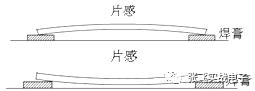
If chip sensor generates a lot of internal stress during manufacturing process, and measures to eliminate this stress are not taken during reflow soldering process, adhered chip sensor will form a vertical film due to influence of internal stress, commonly known as tombstone effect.
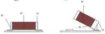
To judge high internal stress in flakes, you can use a simpler method: take hundreds of flakes, put them in a conventional oven or low temperature oven, heat to about 230 ° C, hold heat and observe internal condition of oven. If you hear a beep or even sound of a jumping film, it means that there is a lot of internal stress in product.
▶Component Deformation
If sheet product is bent and deformed, it will have a strengthening effect during welding.
Bad soldering, virtual soldering:
Normal welding:
Wrong site design:
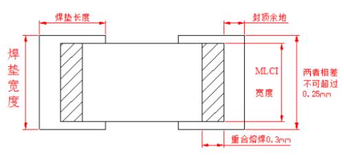
MLKI elements after welding:
a. The two ends of pad must be symmetrical to avoid different sizes, otherwise melting time and wetting force at both ends will be different
b. The welding length exceeds 0.3mm (i.e., overlap length of metal end and pad)
c. The length of contact pad should be as short as possible, usually not more than 0.5 mm.
g. The width of spacer itself should not be too large, and its reasonable width should not exceed 0.25 mm compared to width of MLCI
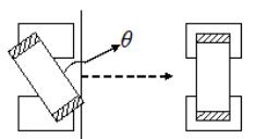
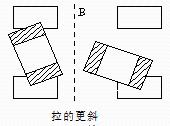
▶Bad Patch
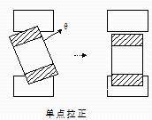
When patching, solder pad roughness or solder paste slipping will shift feel of chip by θ. Due to wetting force that occurs when gasket melts, above three situations may occur, among which self-leveling is main one, but sometimes there will be more oblique pulling or a straightening situation at one point, and chips feel pulled one pad up, even being pulled up, standing obliquely or vertically (tombstone phenomenon). The current placement machine with visual detection of theta angle offset can reduce number of such failures.
▶Soldering temperature
The soldering temperature curve of reflow soldering machine should be set according to requirements of solder. Attempt should be made to melt solder at both ends of chip at same time to avoid difference between two ends of wetting force, which will cause chip to move during soldering process. If there is bad soldering, you can first check whether temperature of reflow soldering machine is abnormal or solder has changed.
Inductors are easily damaged in event of rapid cooling, rapid heating or partial heating, so special attention should be paid to controlling welding temperature during welding and minimizing the welding contact time.
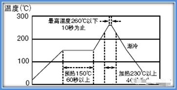
Recommended temperature curve for reflow soldering
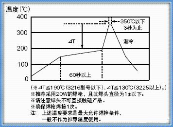
Recommended temperature curve for hand soldering
04 Get in car and open path
▶False welding, poor welding contact
Remove IC sensor from circuit board to check normal operation of IC sensor
▶Current Burn
If chip inductor is selected, rated current of magnetic bead is small or there is a large inrush current in circuit, which will cause current to burn out, chip sensor or magnetic bead to fail, and circuit will open. Remove chip test from PCB, chip fails, and sometimes there are burn marks. If an ongoing burn occurs, number of defective products will be higher, and number of defective products in same batch usually reaches more than one hundred percent.
▶Broken Solder
Rapid cooling and rapid heating during reflow soldering will induce stress inside chip, resulting in a very small number of defects in chip that may have potential open circuits inside, resulting in an open circuit in chip. Remove chip sensitivity test from PCB and it fails. If there is an open welding circuit, number of defective products is usually small, and defective products in same lot usually have less than a thousand varieties.
05 Broken Magnet
▶Magnet Strength
The ceramic package is not strong enough and brittle due to poor sintering or other reasons, ceramic package is damaged when chip is placed or external forces are applied to product
▶Adhesion
If adhesion of silver layer of chip terminal is poor, during reflow soldering, chip sensor is rapidly cooled and heated, thermal expansion and contraction will cause stress, and ceramic body will be subjected to external forces, which may cause chip terminal and porcelain body to separate and fall off or pad is too large, during reflow soldering, wetting force generated by melting of solder paste and reaction of terminal exceeds adhesion of terminal, resulting in damage to terminal.
The chip appears to be burnt or unfinished, or micro-cracks form inside during manufacturing process. Rapid cooling and rapid heating during reflow soldering will cause stress inside chip, crystal cracks or microcracks will expand, causing damage to porcelain body.
4 Semiconductor failure analysis
Failure analysis of semiconductor devices is to determine form of device failure (failure type) by performing various tests and physical, chemical and metallographic tests of failed device, as well as analyzing physical and chemical processes (failure mechanism) that cause failure. device breaks down.Causes of device failure, formulate corrective and improvement measures. Strengthening failure analysis of semiconductor devices and improving their inherent reliability and operational reliability is most active and fundamental way to improve quality of electronic products, and plays a very important role in improving reliability of whole machine.
Use-related semiconductor device failures are very common and account for vast majority of all device failures. Compared with domestic devices, proportion of device failures caused by inherent defects of imported devices is much lower, indicating that imported devices have better process control and a higher level of intrinsic reliability.
01 Usage related disappearance
The main causes of failure related to use are: damage from excessive electrical voltage, electrostatic damage, incorrect device selection, incorrect circuit design, mechanical overvoltage, operational errors, etc.
▶Electric shock
Failure caused by electrical overload is cause of vast majority of failures in used devices. This happens at various stages of testing, verification, installation, debugging and operation of devices. Specific reasons may vary. common is caused by excessive bridge short circuit, electrical surge caused by ground wire and power supply system, soldering iron leakage, induced electrical surge caused by improper grounding of instruments or test benches, etc. short circuit of metal bridge, as well as instantaneous high-current electrical voltage created by recoil electromotive force of coil, and high-voltage and low-current electrical voltage caused by leakage and induction; According to device, there are PN junction failures and plating burn-in directly caused by external overvoltage, and burn-in failure caused by external overvoltage, PN junction damage triggering a CMOS circuit short circuit and an increase in power supply current.
▶Electrostatic Damage
Strictly speaking, electrostatic damage to devices also refers to surge damage, but due to nature of electrostatic overvoltage and widespread use of electrostatic sensitive devices, this problem is becoming more and more urgent. Characteristics of electrostatic superelectric voltage: high voltage (hundreds of volts to tens of thousands of volts), low energy, large instantaneous current, but extremely short duration. Compared to general stress from overexertion,electrostatic damage often occurs in non-voltage processes such as transportation, transfer and installation of device, it is not related to device damage process and is very harmful. In terms of failure modes after electrostatic damage to devices, there are not only high voltage, low current failure modes, such as PN junction failure and flashover, but also high current failure modes, such as plating and polysilicon burnout.
▶Wrong device selection
Incorrect device selection is also one of causes of failures often encountered with usage problems. The main reason is that developers do not have a comprehensive understanding of parameters and performance of device and do not think carefully, and selected devices cannot meet requirements. designed circuit in some aspects.
▶Operation failed
Mistakes in operation are also one of common causes of device failure, such as a write failure caused by reversed device polarity.
02 Crash caused by internal device defects
The failure reasons related to internal defects of device mainly include: surface problems, plating problems, wire connection problems, chip connection problems, packaging problems, internal defects, etc. Among these reasons, failures, caused by surface problems, adhesion problems, and chip sticking problems have a greater impact on reliability of device, and all of them are intermittent and often repeated.
▶Surface Issues
In terms of reliability, charge of mobile positive ions in silicon dioxide layer has greatest impact on device, which reduces breakdown voltage of device, increases leakage current, and increases power-on time. Gradually reduce device performance. Devices with such defects cannot be eliminated by conventional testing methods, which is very detrimental to reliability. In addition, micro-holes in silicon dioxide layer on chip surface have a greater impact on device reliability. Devices with such defects often have a very thin oxide layer at beginning of pinhole. Device performance remains normal, lapping, shielding and other tests can pass smoothly, but after prolonged use due to TDDB effect and power surge. Hitting pin hole will cause a short circuit, causing device to fail.
▶Problems with plating
Common plating problems that lead to device failure include aluminum step failure, aluminum corrosion, metal film scratches, etc. For primary integrated circuits, aluminum step failure and aluminum corrosion are more common; Forsecondary integrated circuits, open circuit failure caused by scratching of internal metal film resistors during cleaning and wiping is also a common failure mode.
▶Problems with clamp wire connection
Common faults caused by wiring problems are listed below.
(1) The end of welding wire or weld is contaminated and corroded, causing weld to fall off or corrode, resulting in an open circuit.
(2) The gold layer under external pressure solder joint is not fixed securely, or gold-aluminum alloy occurs, causing pressure solder joint to fall off.
(3) The pressure welding point is overpressure welded, causing neck of welding wire to detach and break circuit.
(4) The curvature of connecting wire is not enough, and angle between connecting wire and surface of chip is too small, and it is easy to collide with edge of silicon chip or metallized aluminum wire under connecting wire, causing device to fail.
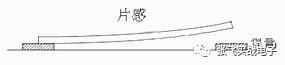
▶Die bonding problems
The most common occurrence is open circuit caused by insufficient solder to bond chips, solder oxidation, and low sintering temperature. The adhesion of chip is poor and solder oxidizes and blackens, causing chip to lift up and separate from base after being mechanically affected during "magnetic forming", resulting in failure when circuit breaks.
▶Encapsulation issues
Errors Caused by Encapsulation Problems There are following kinds of effects.
(1) The packaging is poor, sheath is leaking, so that water vapor or corrosive substances enter inside of sheath, causing corrosion of connecting wire and plating.
(2) There is a defect in tube body that causes tube leg to open and cause a short circuit.
(3) The inner coating is cracked and connecting aluminum wire is broken, resulting in an open circuit or instant failure of device. This failure phenomenon often occurs when device is subjected to high and low temperature tests.
▶Body Defect
Defects in package of semiconductor devices can also cause transient characteristics of device to deteriorate and fail, resulting in a fire.
Related
- Haberdashery|General failure mechanism and analysis of electronic components
- Experience in recognition of circuit diagrams of electronic circuits and method of circuit analysis
- Analysis of damping RC circuit of a switching power supply "haberdashery"
- What does inside of a multilayer PCB look like? Three-dimensional general analysis of design process of high-quality printed circuit boards
- Comprehensive MLCC Failure Analysis
- ADC basics and comparative analysis of different ADC technologies
- Analysis and comparison of 6 most commonly used DC power supply circuits
- A list of some of the tools commonly used by electronic engineers.
- Principle of electronic switch to realize overcurrent protection
- An interesting summary of PID algorithm full of haberdashery
Hot Posts
 How to distinguish induction from leakage, we will teach you three tricks! Ordinary people can also learn super practical
- What is drowning in gold? Why Shen Jin?
- This is a metaphor for EMI/EMS/EMC that can be understood at a glance.
- How many types of pads have you seen in PCB design?
- Summary of Common PCB Repair Techniques
- What is three anti-paint? How to use it correctly?
- Knowing these rules, you will not get confused looking at circuit diagram.
- How to make anti-interference PCB design?
- Can diodes do this?