Location:Home Page > Archive Archive
Detailed explanation of 3 classic topologies (with circuit diagrams and calculation formulas)
2023-08-29【Archive】
This article will detail various aspects of buck, boost, and buck-boost topologies.
Dollar Converter
In fig. 1 is a diagram of an asynchronous buck converter. A buck converter steps down input voltage to a lower output voltage. When switch Q1 is turned on, power is transferred to output.
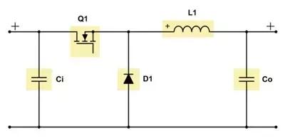
Figure 1. Schematic diagram of an asynchronous buck converter
Formula 1 calculates duty cycle:
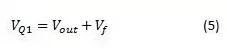
Equation 2 calculates maximum MOSFET voltage:
Equation 3 gives maximum diode load:
Where Vin is input voltage, Vout is output voltage, and Vf is forward voltage of diode.
The greater difference between input and output voltage, more efficient buck converter is compared to a linear or low dropout (LDO) regulator.
Although input of buck converter is pulsed current, output current is continuous due to inductor-capacitor (LC) filter at output of converter. As a result, voltage ripple reflected at input will be greater than ripple at output.
For low duty cycle buck converters with more than 3A output current, a synchronous rectifier is recommended. If your power supply requires an output current greater than 30A, poly-phase or interleaved power stages are recommended as this minimizes stress on components, spreads generated heat across multiple power stages, and reduces input ripple reflections to converter.
The use of an N-FET creates a duty cycle limitation as bootstrap capacitor needs to be recharged on every switching cycle. In this case, maximum fill factor is in range of 95-99%.
The buck converters usually have good dynamic performance because they have a direct topology. The achievable bandwidth depends on quality of error amplifier and selected switching frequency.
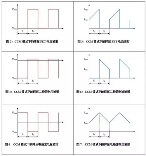
Figures 2-7 show voltage and current waveforms of a FET, diode, and inductor in continuous conduction mode (CCM) in an asynchronous buck converter.
Boost Converter
The boost converter boosts input voltage to a higher output voltage. When switch Q1 is turned off, energy is transferred to output. On fig. 8 is a schematic diagram of a non-synchronous boost converter.
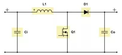
Figure 8: Schematic diagram of an asynchronous boost converter
Formula 4 calculates duty cycle:
Equation 5 calculates maximum MOSFET voltage:
Equation 6 gives maximum diode load:
Where Vin is input voltage, Vout is output voltage, and Vf is forward voltage of diode.
When using a boost converter, you can see a pulsed output current because there is an LC filter at input. Therefore, input current is continuous and output voltage ripple is larger than input voltage ripple.
When designing a boost converter, it is important to know that there is a constant connection between input and output, even when converter is not switching. Measures must be taken against a possible short circuit at output.
For output currents greater than 4 A, a synchronous rectifier should be used instead of a diode. If power supply needs to provide an output current greater than 10 A, it is highly recommended to use multi-phase or alternating power stages.
When operating in CCM mode, dynamic performance of boost converter is limited due to zero in right half-plane (RHPZ) of its transfer function. Since RHPZ cannot compensate, achievable bandwidth is typically between one-fifth and one-tenth of the RHPZ frequency. See Equation 7:
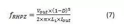
Where Vout is output voltage, D is duty cycle, Iout is output current, and L1 is inductance of boost converter.
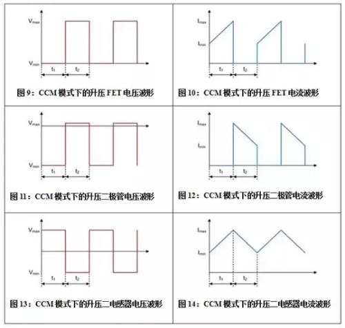
In fig. Figures 9-14 show voltage and current waveforms of a FET, diode, and inductor in an asynchronous boost converter in CCM mode.
Up/down converter
The buck-boost converter is a combination of buck and boost power stages with same choke. See fig. 15.
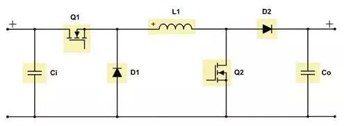
Figure 15. Schematic diagram of a two-switch buck-boost converter
The buck-boost topology is useful because input voltage can be less than, greater than, or same as output voltage, with required output power exceeding 50W.
For output power less than 50W, single-ended primary inductance converter (SEPIC) is a more economical option because it uses fewer components.
When input voltage is greater than output voltage, buck-boost converter operates in buck mode; when input voltage is less than output voltage, it works in boost mode.
When converter operates in transmission region where input voltage is within output voltage range, there are two concepts for handling such situations: either buck and boost stages are active at same time, or switching cycle is between buck and boost stages, both of which normally work at half normal switching frequency.
The second concept may cause sub-harmonic noise at output, and accuracy of output voltage may not be as accurate compared to a conventional buck or boost converter, but converter will be more accurate than first concept.
In a buck-boost topology, surge currents are present at both input and output because there is no LC filter in either direction.
For buck-boost converters, separate buck and boost stage calculations can be used.
Double switch buck/boost converter for power range from 50W to 100W (similar to LM5118) and synchronous rectification up to 400W (similar to LM5175). A synchronous rectifier with same current limit as non-combined buck and boost power stage is recommended.
You need to design a buck/boost compensation network for boost stage, as RHPZ will limit regulator's bandwidth.
Related
- Detailed explanation of 3 classic topologies (with circuit diagrams and calculation formulas)
- Experience in recognition of circuit diagrams of electronic circuits and method of circuit analysis
- A detailed explanation of role of pull-up resistors on triodes and MOS lamps.
- [Comic] Detailed explanation of knowledge of power sources
- Analysis of power circuit of a classic single-chip microcomputer
- What is a delay scheme? Explanation of 6 Kinds of Delay Circuit Principles
- A detailed explanation of three commonly used LED drive power schemes.
- Hardware Collection: 50 Common Circuit Diagrams
- Three circuit diagrams to teach you how to understand how a buck RC works
- You must learn drawing techniques and skills of 18 special circuit board routes.
Hot Posts
 How to distinguish induction from leakage, we will teach you three tricks! Ordinary people can also learn super practical
- What is drowning in gold? Why Shen Jin?
- This is a metaphor for EMI/EMS/EMC that can be understood at a glance.
- How many types of pads have you seen in PCB design?
- Summary of Common PCB Repair Techniques
- What is three anti-paint? How to use it correctly?
- Knowing these rules, you will not get confused looking at circuit diagram.
- How to make anti-interference PCB design?
- Can diodes do this?