Location:Home Page > Archive Archive
Comprehensive MLCC Failure Analysis
2023-03-18【Archive】
Q: What is structure of MLCC capacitor??
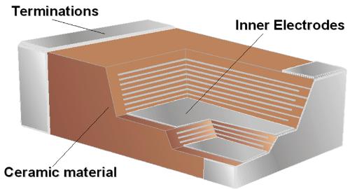
A: Multilayer ceramic capacitors are laminated with a ceramic dielectric diaphragm with printed electrodes (inner electrodes) by a dislocation method and sintered at high temperature to form a ceramic chip. capacitor is sealed with a metal layer (outer electrode).
MLCC properties:
Mechanical strength: hard and brittle, this is a characteristic of mechanical strength of ceramic materials.
Hot brittleness: The internal stresses of MLCC are very complex, so ability to withstand thermal shock is very limited.
Q: What are common failure modes for MLCC capacitors?
About:
QuestionHow to distinguish defects from different causes? What are precautions?
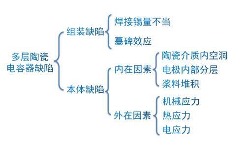
Assembly defect
1. Incorrect amount of solder tin
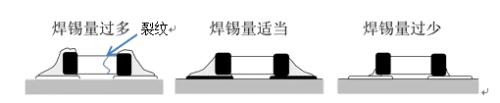
Figure 1. Schematic diagram of capacitor solder volume
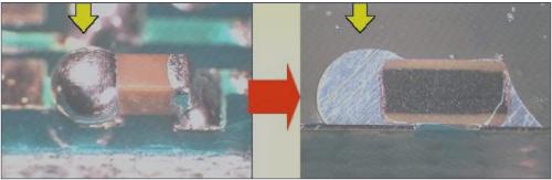
Fig. 2. Too much solder causes capacitor to crack
When temperature changes, an excessive amount of solder will create a high voltage on capacitor die, which will cause capacitor to break internally or remove capacitor cover. The crack usually occurs on side with less solder; too little solder can cause welding strength Insufficient, capacitor is disconnected from circuit board, causing an open circuit.
2. Gravestone effect
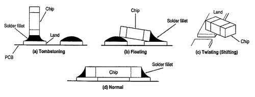
Figure 3. Schematic diagram of tombstone effect
During reflow soldering, unbalanced surface tension of electrodes at both ends of chip component, after solder melts, creates a torque that pulls on one end of component, forming a virtual solder. torque is large, one end of component will be pulled up. Create a tombstone effect.
Reason: Large difference in electrode sizes at both ends, tinning is uneven, PCB pads are different sizes, there is dirt or moisture, oxidation and buried holes in pads; solder paste. If viscosity is too high, tin powder will be oxidized.
Action:
①Clean and dry PCB before welding to remove surface dirt and moisture;
②Please check before soldering to make sure left and right pads are the same size;
③Solder paste must not be applied for too long, it must be thoroughly mixed before soldering.
Ontological defects — internal factors
1. Holes in ceramic media
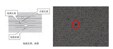
Figure 4. Hollow diagram of a ceramic dielectric
Reason:
① Impurities are adsorbed on surface of dielectric diaphragm;
② Impurities are mixed during electrode printing process;
③Suspension of inner electrode is mixed with impurities or dispersion of organic matter is uneven.
2. The inner layer of electrode
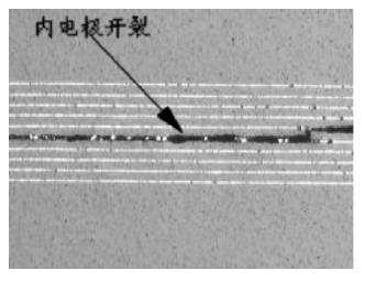
Fig. 5. Inner layers of electrodes
Reason: Multilayer ceramic capacitor sintering is stacking and co-firing of multilayer materials. The shrinkage rate of ceramic film and internal paste during debinding and sintering process is different. In process of sintering into ceramic, stress is generated inside chip, which causes MLCC to re-lamination.
Precautions: When manufacturing MLCC, using an internal slurry that works better with porcelain powder can reduce risk of delamination and cracking.
3. Manure accumulation
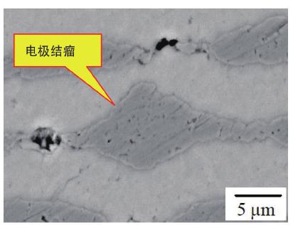
Figure 6. Sludge accumulation defects
Reason:
① The metal particles in inner suspension are unevenly distributed;
② The local seal of inner electrode is too thick;
③ The quality of inner electrode paste is not very good.
Ontological defects — external factors
1. Stress crack
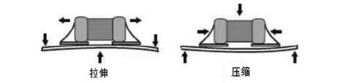
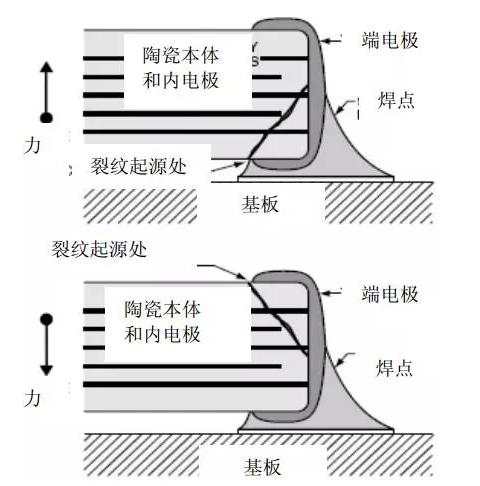
Figure 7. Schematic diagram of MLCC stress cracking
Reason: Multilayer ceramic capacitors are characterized by their ability to withstand high compressive stresses, but have relatively low bending resistance. When PCB bends and deforms, MLCC ceramic substrate will not bend with board, and stress on long side is greater than on short side. When stress exceeds strength of MLCC ceramic package, bending cracks will appear. When a capacitor is subjected to excessive mechanical stress, 45-degree cracks and Y-shaped cracks usually form in it.
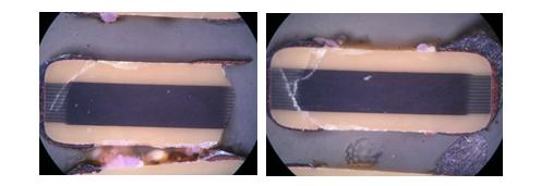
Fig. 8. Typical mechanical crack capacity
Common voltage sources: PCB operation during process, factors such as people, equipment and gravity during circulation process, insertion of through components, circuit testing, single board segmentation, etc. PCB assembly; printed circuit board rivet; mounting with screws, etc.
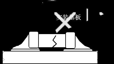
Figure 9. Schematic diagram of stress cracking during circulation
Action:
①Choose appropriate PCB thickness.
② When calculating degree of bending of PCB, consider amount of bending that MLCC can withstand. Heavier components should be placed as evenly as possible to reduce board gravity bending during manufacturing.
③Optimize position and direction of MLCC on PCB to reduce mechanical stress it puts on PCB. The MLCC should try to maintain a certain distance from auxiliary holes and cutting lines or grooves in PCB so that board is subjected to the least bending tensile stress after installation.
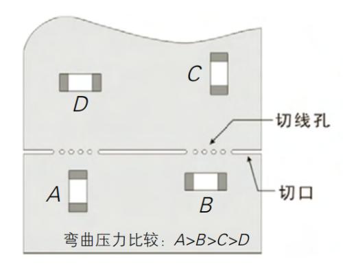
Fig. 10. Comparison of voltage distribution on a printed circuit board
④The mounting direction of MLCC should be parallel to hole, cut line, or groove to ensure uniform tensile force on MLCC when PCB is bent and prevent damage during cutting.
⑤ Try not to place MLCC near screw hole to prevent cracking on impact when screw is tightened. Where capacitance needs to be placed, lead-encased capacitors can be considered.
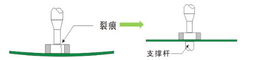
Figure 11 Schematic diagram of rational use of support rods
⑥ Use support frame wisely during test to avoid bending board under force.
2. Thermal stress crack
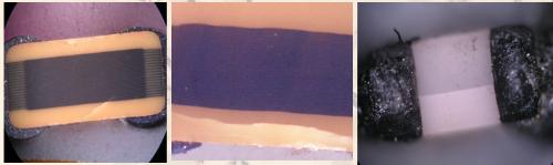
Figure 12. Typical capacitor cracking under thermal stress
When a capacitor is subjected to excessive thermal stresses, resulting cracks do not have a fixed shape and can be distributed over different cut surfaces. In severe cases, horizontal cracks form on side of condenser.
Reason: The formation of thermal stress cracks and poor resistance of capacitor itself to heat of welding are due to introduction of thermal shock into manufacturing process. Possible reasons: incorrect soldering iron rework, unstable SMT furnace temperature, furnace temperature curve change rate too fast, etc.
Measures:①The processing method should take into account temperature characteristics and size of MLCC. Large size MLCCs above 1210 may cause uneven heating and breaking voltage, so wave soldering cannot be used;< / p >
② Pay attention to temperature curve setting of welding equipment. When setting parameters, temperature jump should not exceed 150 ° C, temperature change should not exceed 2 ° C / s, and preheating time should be more than 2 minutes After welding, there should be no auxiliary cooling equipment. be used and it must cool naturally with temperature of oven.
③Before hand soldering, a preheating process should be added before soldering. During whole hand soldering process, soldering iron tip is prohibited from directly contacting capacitor electrodes or case. Re-soldering should be carried out after soldered joint has cooled down, and number of times should not exceed 2 times
3. Electrical stress crack
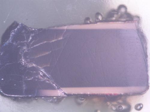
Figure 13. Typical capacitor cracking under electrical stress
Overvoltage leads to irreversible changes in product, manifested in form of breakdown of withstand voltage, and in severe cases leads to serious consequences, such as cracking, explosion and even fire of multilayer ceramic capacitors. In MLCCs subjected to excessive electrical stress, cracks propagate explosively from within.
Measures:①When choosing a device, please note that actual operating voltage cannot be higher than rated operating voltage of device;
② Avoid exposing device to power surges and static electricity.
Question. How to perform MLCC failure analysis?
A: The whole process is divided into 5 main steps: appearance inspection, electrical measurement analysis, non-destructive analysis, destructive analysis, component analysis, and appearance inspection and electrical testing. process, internal structure inspection, failure point location, failure cause analysis, failure point local component analysis, failure analysis process of entire MLCC is shown in figure:

Fig. 14. Flowchart of MLCC Failure Analysis
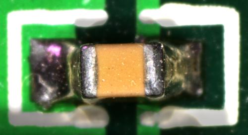
Fig. 15. Observation of a stereoscopic image using a digital microscope with super depth of field
Firstly, use a digital microscope with an ultra-high depth of field to view appearance in three-dimensional space, check whether there are cracks on surface of capacitor, and check rise of solder on output side from several angles. The capacitor looks good, there are no external cracks, solder climbs well.
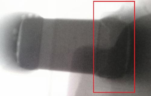
Figure 16. X-ray control
X-ray examination of failed capacitor revealed a crack on right side of the capacitor.
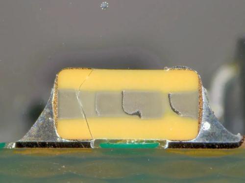
Figure 17. Cross section of a digital microscope with an ultra-deep field of view for section analysis.
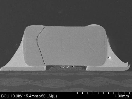
Figure 18. Fracture morphology in SEM observation section.
On metallographic section of capacitor, it is clearly seen that internal cracks of capacitor occur near weld end, which has shape of letter Y. This is a typical form of crack under mechanical stress. Check possible voltage sources and standardize workflow, and finally solve problem of capacitor cracking.
Related
- Comprehensive MLCC Failure Analysis
- Haberdashery|General failure mechanism and analysis of electronic components
- Surprisingly, this is most prone to PCB failure?
- Several Effective Circuit Analysis Techniques
- Suggested collection: Capacitor filtering analysis and EMC suggestions.
- Senior engineer summarizes 10 methods for complex circuit analysis
- ADC basics and comparative analysis of different ADC technologies
- Analysis of power circuit of a classic single-chip microcomputer
- List of 5 Most Practical Network Analysis Techniques! must watch
- Circuit Analysis of 6 Examples Explaining Lightning Surge Protection in Detail
Hot Posts
 How to distinguish induction from leakage, we will teach you three tricks! Ordinary people can also learn super practical
- What is drowning in gold? Why Shen Jin?
- This is a metaphor for EMI/EMS/EMC that can be understood at a glance.
- How many types of pads have you seen in PCB design?
- Summary of Common PCB Repair Techniques
- What is three anti-paint? How to use it correctly?
- Knowing these rules, you will not get confused looking at circuit diagram.
- How to make anti-interference PCB design?
- Can diodes do this?