Location:Home Page > Archive Archive
Why doesn't a push-pull gate type circuit use a top P and a bottom N?
2023-04-13【Archive】
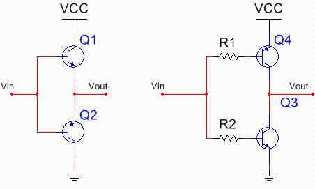
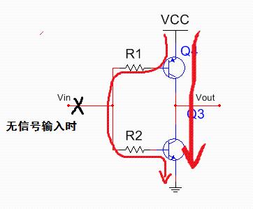
In signal control and driving, a push-pull scheme is often used to speed up control. A push-pull circuit can be composed of two structures: top P and bottom N and top N and bottom P. Its circuit diagram is shown below.
In normal times, push-pull circuit, which I personally often encounter, is first. Every time I ask engineers around me, "Why don't you use second type? The second type is upper P-lower N-type. theory." But in practice, no one has ever answered me positively why upper P less than N is not applicable. Perhaps many people will bother answering this question, but this is really a question that almost beginners in electronic design will consider. Today I will deal with this little problem.
Let's look at top type N and bottom P first. From circuit diagram, we can know that phases of output signal and input signal are same, that is, input signal is high. Output is high. However, according to performance characteristics of tube, N is tube output voltage amplitude N = Vb = 0.7 V, so output amplitude of modified model will be limited by output signal. Therefore, requirements for amplitude of input signal are relatively strict, otherwise high-level signal of subsequent stage may not be high enough.
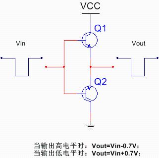
The operation diagram of its output is shown in figure above. Attentive people may find that when high level of input signal is lower than supply voltage, it means that upper tube CE node N will withstand a higher voltage. This also means that top tube will be at risk of heat damage.
There is some truth in this conclusion, but in practice, when push-pull circuit performs signal driving, current flowing through it will not be very large, so in this case top tube is not easily damaged. However, if push-pull circuit is used to control load, a large current will flow through tube at this time. If input signal amplitude is small at this time, heat generated by top tube will be very serious. Of course, when low level of input signal is higher than reference voltage, down tube P will also have same problem.
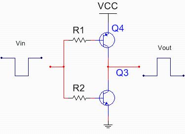
For a model with top P and bottom N, from schematic diagram, we can know that output and output of model are reversed. That is, when input is high, output is low.
In a real applied circuit, we can compare it to top N-bottom P model. After comparison, it can be found that triode base of upper model P with lower N will have a resistor in series, but upper N with lower P can be omitted in practical applications. The reason for adding these two resistors to top P and bottom N model is to isolate top tube P and bottom tube N to isolate signal. If signal isolation is not performed, it can be seen from schematic that top tube signal P will actually affect bottom tube N.
It can be seen from above diagram that when tube P is turned on, its signal will pass through tube N, resulting in a collusion problem between tubes P and N. So resistor cannot be saved. Many people may think that adding two resistors is worth nothing, but if this is put into production, if price of a resistor is 0.1 cents, then production of 10 million units means that "because of these two resistors, cost will directly increase. Ten thousand yuan."
Also, we often think that after adding a resistor, everything will be fine, but it is not. Although resistor is added, we must strictly ensure that there is always a signal at input terminal and signal amplitude is high enough, otherwise it will also cause collusion problem.
However, even if it can be guaranteed that amplitude of control signal will be high enough, when signal undergoes a high-to-low transition, it must pass through signal transition interval, which means that when signal transitions, there will still be problems collusion. To solve this problem, slew rate of control signal is required to be much larger than turn-on time of triode (i.e., control signal has completed signal conversion before triode reacts to switching to avoid collusion).
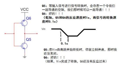
You can check switching time of a general purpose triode. After checking, you may find that requirements for push-pull circuit of upper P lower N-type are too stringent.
Summarizing, we often choose upper N lower P type in practical applications. The following table shows characteristics of two models for reference:
Of course, upper P model of lower N has so many disadvantages only in gate type (that is, triode model), and it is still very popular in field effect transistor (MOSFET). Specific reasons can be found according to your interests.
Related
- Why doesn't a push-pull gate type circuit use a top P and a bottom N?
- A detailed explanation of role of pull-up resistors on triodes and MOS lamps.
- How to design a triode amplifier circuit
- Analysis of power circuit of a classic single-chip microcomputer
- Hardware Circuit Design Specification: A Very Good Reference to Hardware Design
- Analysis of damping RC circuit of a switching power supply "haberdashery"
- Principal analysis of BUCK / BOOST circuit, a summary is also in place
- What is a delay scheme? Explanation of 6 Kinds of Delay Circuit Principles
- Do you know four magical ways to use a digital multimeter?
- What is purpose of connecting a polar capacitor and a non-polar capacitor in parallel?
Hot Posts
 How to distinguish induction from leakage, we will teach you three tricks! Ordinary people can also learn super practical
- What is drowning in gold? Why Shen Jin?
- This is a metaphor for EMI/EMS/EMC that can be understood at a glance.
- How many types of pads have you seen in PCB design?
- Summary of Common PCB Repair Techniques
- What is three anti-paint? How to use it correctly?
- Knowing these rules, you will not get confused looking at circuit diagram.
- How to make anti-interference PCB design?
- Can diodes do this?